

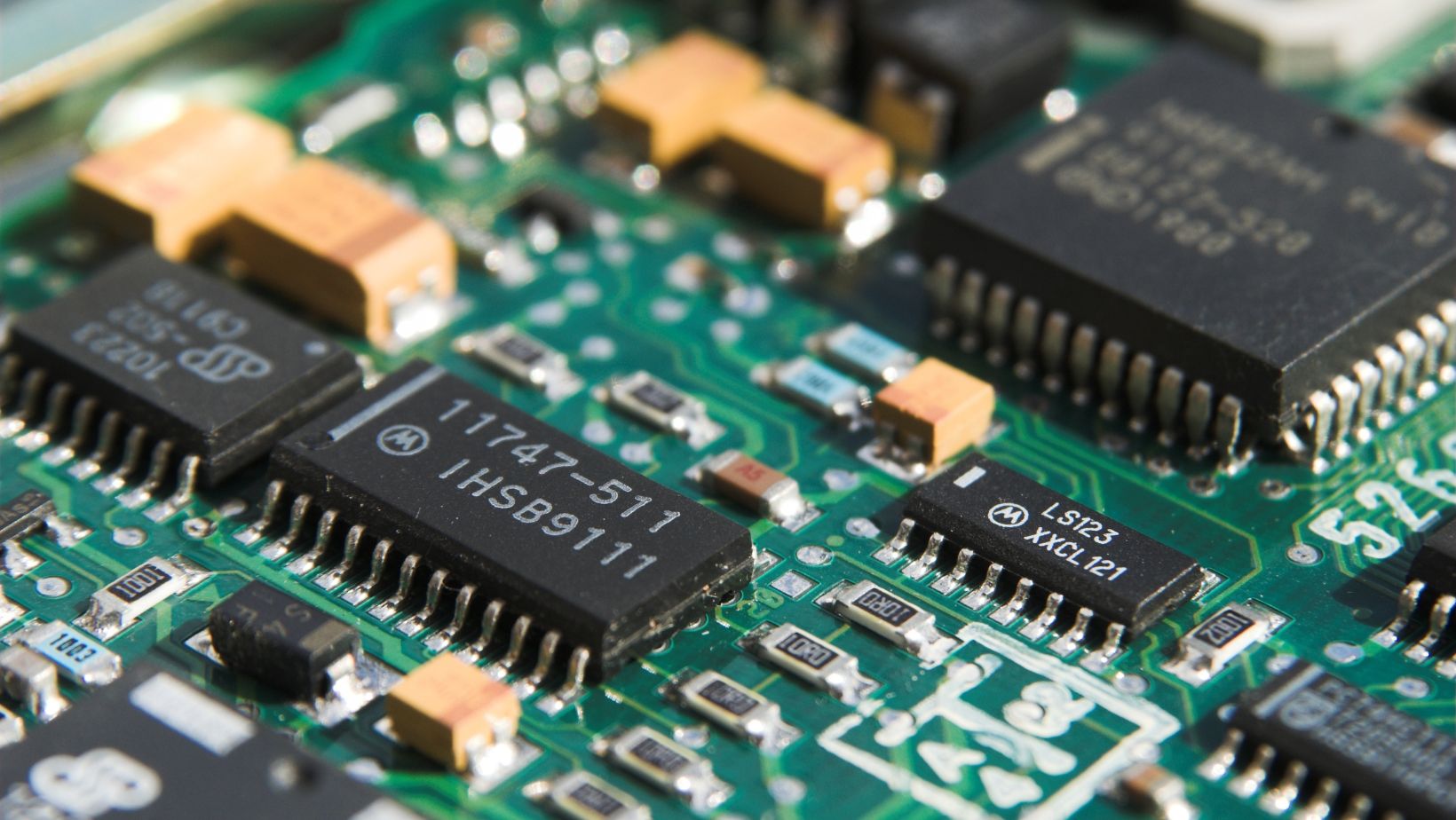
Printed Circuit Boards (PCBs) are considered as the miniature highways for the components and are seen as the central part of present day electronics. Thus, with the electronics industry changing and the emphasis placed on HW development matching SW creation, the knowledge of the PCB fabrication process becomes vital. The following text will be devoted to the detailed description of the main stages of the PCB fabrication. It is hoped that by explaining this process, some understanding into the highly complex area of PCB production and the importance of this industry in the progression of electronic technology, will be gained.
The PCB Fabrication Process: Step-by-Step
PCB fabrication process is a delicate process by which an idea is brought to existence in the form of a circuit that will declare its readiness to host the electronic elements. It is a set of sequential processes each so vital that it determines the final look and quality of the designed end product. It is now time to look into these steps to see how Lion Circuits achieves fast, efficient production of PCBs.
-
Design and Schematic Creation
The detailed steps of PCB fabrication include design. To design a circuit, engineers employ computer aided design tools or CADs to draw what is called a schematic and herein maps out the electrical connections of the circuit. The kind of arrangement requires time and strategy to place the components appropriately and to route the signals in the best way possible.
-
PCB Layout Design
After that, the schematic is ready, which will be further transformed in a physical design. This process entails positioning of parts and drawing characteristics of copper paths that will constitute the required circuit on the board. Some of the aspects that the designers need to take into account include signal integrity, power integrity as well as thermal integrity. Partnering with a PCB design company can help address these challenges through expert placement strategies and signal optimization. Conclusive Tech offers specialized PCB design services that support engineers in creating reliable and production-ready layouts.
-
Design Rule Check (DRC)
As with many other designs before production, there is a Design Rule Check that it goes through. This streamlines IT tasks, and confirms that the layout does not violate manufacturing restrictions as well as norms. Of them they check certain parameters like minimum trace width, distance between the traces, and the clearance between them.
-
Gerber File Generation
The last design is output in Gerber files, or rather, it is converted to Gerber files. These files consist of all the necessary data for production; copper layer topography, solder mask, silkscreen, and drill sites. The organisation of the files thereby means each file is a layer/aspect of a PCB.
-
Photoresist Application
Fabrication process of a PCB starts with a copper-clad laminate. As for the subsequent process, a photosensitive material called photoresist is deposited on both sides of a board.
This cinematography will be the basis for transferring the circuit pattern on the copper into the film.
-
Image Exposure
Gerber files are used to produce the film negatives of each copper layer. These negatives are then transferred over to the photoresist-coated board then exposed to high-intensity ultraviolet light. This process makes the exposed area solidify and the unexposed areas to become soluble in the alkaline developer.
-
Developing
Subsequently the board is dipped in a chemical which dissolves and washes the un-hardened photoresist with the hardened one forming the desired pattern of the circuit.
-
Etching
The board is then exposed to an etching medium depending on the kind of circuit to be made. An etching solution dissolves the copper which is exposed while the copper traces beneath the hard-baked photoresist remain intact. At this step the pattern of the circuit appears on the board having the same look as the diagram.
-
Photoresist Stripping
After etching, the remaining photoresist is removed to show the copper layer which makes the exact circuit.
-
Drilling
Component leads and Via are made on the board through drilling of holes on the board. This is normally done with the help of Computer Numeric Controlled (CNC) drilling machines that perform the instructions found in the Gerber files.
-
Plating
The drilled holes are also reinforced with copper, in order to form a working electrical connection between the layers. This process may also involve electroless copper deposition for plate uniform thickness.
-
Solder Mask Application
To completely protect the copper surface, a layer of solder mask is applied to the board. It also shields the copper traces and does not allow the solder to solder between connected points. It imparts greenish colour to PCBs although they can also be produced in other colours.
-
Silkscreen Printing
Originally only the text and the symbols to be imprinted on the board are printed on the board surface by silkscreen methods. This provides component designators, logos and other marks, which are useful in assembly of the products and identification respectively.
-
Surface Finish
An outer layer is used to cover exposed copper as well as improve the ability to solder to the material. Some of the regular ones are hot air solder levelling, electroless nickel immersion gold, and organic solderability preservation.
-
Electrical Testing
The electrical checks performed on every board include compact checking of all connections, shorts, or opens. This can be a fully automated test equipment or a flying probe tester.
-
Cutting and Shaping
When many PCBs are produced on a single panel, they are severed by either routing machines or by the use of break-away tabs. The boards are sanded to its final thickness and dimension.
-
Final Inspection
The physical characteristics and any imperfections are examined with thorough visual aids used in the inspection.
This may for example be in the form of automated optical inspection (AOI) for volume production lines.
-
Packaging and Shipping
The finished PCBs are secured in an appropriate manner to prevent physical harm and static electricity. They are delivered to the consumer or transferred to the assembly line if the manufacturer also sells components.
Conclusion
PCB fabrication can be described as a scientific endeavor that involves accurate articulation of the desired design and sophisticated assembly work. Of course, Lion Circuits’ software-driven manufacturing approach does not only improve this process, but the flexibility and scalability at the same time. Overall, PCB fabrication is a set of processes, the detailed analysis of each of which will significantly help developers and engineers to avoid many critical mistakes and achieve maximum performance.
Taken together, the creation of a PCB starts with a conceptual design and includes such steps as proper planning, precise and detailed implementation, and clear testing. Lion Circuits is paving ways in this area where more often software developers want to work with truly expert electronics manufacturing, especially with short lead times.
Understanding the various aspects of the manufacturing of PCB’s means that dreams and inventions can be applied to reality through the advancement of technology.

